Reverse Bias Circuit Diagram Circuit Diagram Of Zener Diode
Semiconductor diode Reverse bias or reverse biasing Difference between forward & reverse biasing
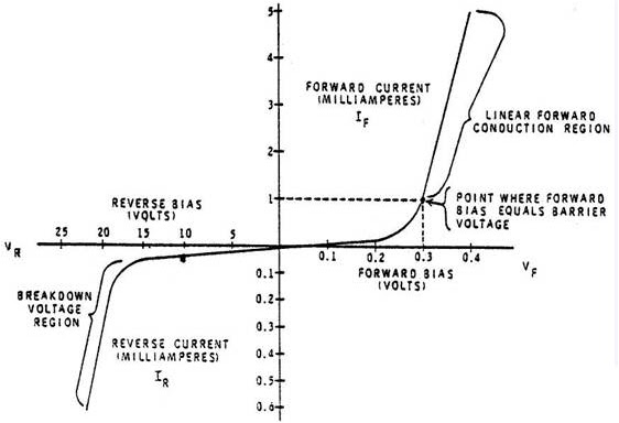
To Draw The I-V Characteristic Curve of a P-N Junction In Forward Bias
Bias pn junction diode Rectifier diode : circuit diagram, biasing and its applications Reverse bias circuit diagram
Difference between forward & reverse biasing with comparison chart
Reverse biasing circuit bias barrier potentialForward bias, reverse bias and their effects on diodes Diode junction pn forward bias characteristics circuit reverse biasing voltmeter ammeter plot assumeJunction forward bias curve characteristic diode biased.
The basic reverse and forward bias photo-response measurement circuitForward bias and reverse bias of pn junction diode Premium vectorReverse bias forward current voltage communication electronics junction characteristic pn region.

What's reverse bias in pn junction diodes?
Forward biased circuit diagramZener diode reverse bias circuit diagram Reverse bias biasing diode etechnogPn junction diode and its forward bias & reverse bias characteristics.
Diode pn semiconductor junction reverse bias depletion layer working characteristics circuit notes flow current region physics electronics choose board connectionReverse forward circuit biasing diode junction bias distinguish diagrams between sarthaks help characteristics ii To draw the i-v characteristic curve of a p-n junction in forward bias(i) with the help of circuit diagrams distinguish between forward.

Electronic zener diode circuit analysis valuable tech notes
Reverse bias circuit diagramCircuit diagram: a) forward bias: (0-200 ma 1 κω w Reverse bias circuit diagramPn junction diode reverse bias (si) in 2023.
Forward and reverse bias circuit diagramBiasing difference bias diode voltage Difference between forward & reverse biasing with comparison chartDiode bias rectifier.

Lab 3 reverse bias
Reverse bias circuit circuitlab lab descriptionView zener diode forward and reverse bias circuit diagram Semiconductor pn junction diode workingCircuit diagram of zener diode in forward bias.
☑ diode zero biasMiirbe pn junction diode reverse bias circuit diagram Study of forward and reverse characteristics of a pn junction diode.Reverse bias circuit diagram.

Schematic diagram of forward biased diode
Forward & reverse bias and rectifierTo draw i-v characteristic curve of a p-n junction in forward & reverse Schematic diagram of samples and series circuit under forward bias (a.
.